
AlixLabs
@AlixLabs
Followers
90
Following
145
Statuses
122
Atomic Level Fragmentation #ALEtch
Lund, Sverige
Joined June 2019
Yay! We made the SEMI-final! ;-)

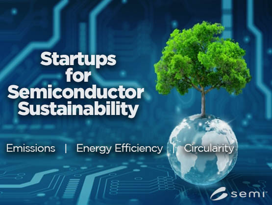
The SEMI #Startups for #Semiconductor #Sustainability program has announced 2023 semifinalists, organizations that will focus on three areas: #circularity, #emissions and #energy efficiency. Learn more about our work to spur more green tech innovation 👉
0
0
4
2
1
11
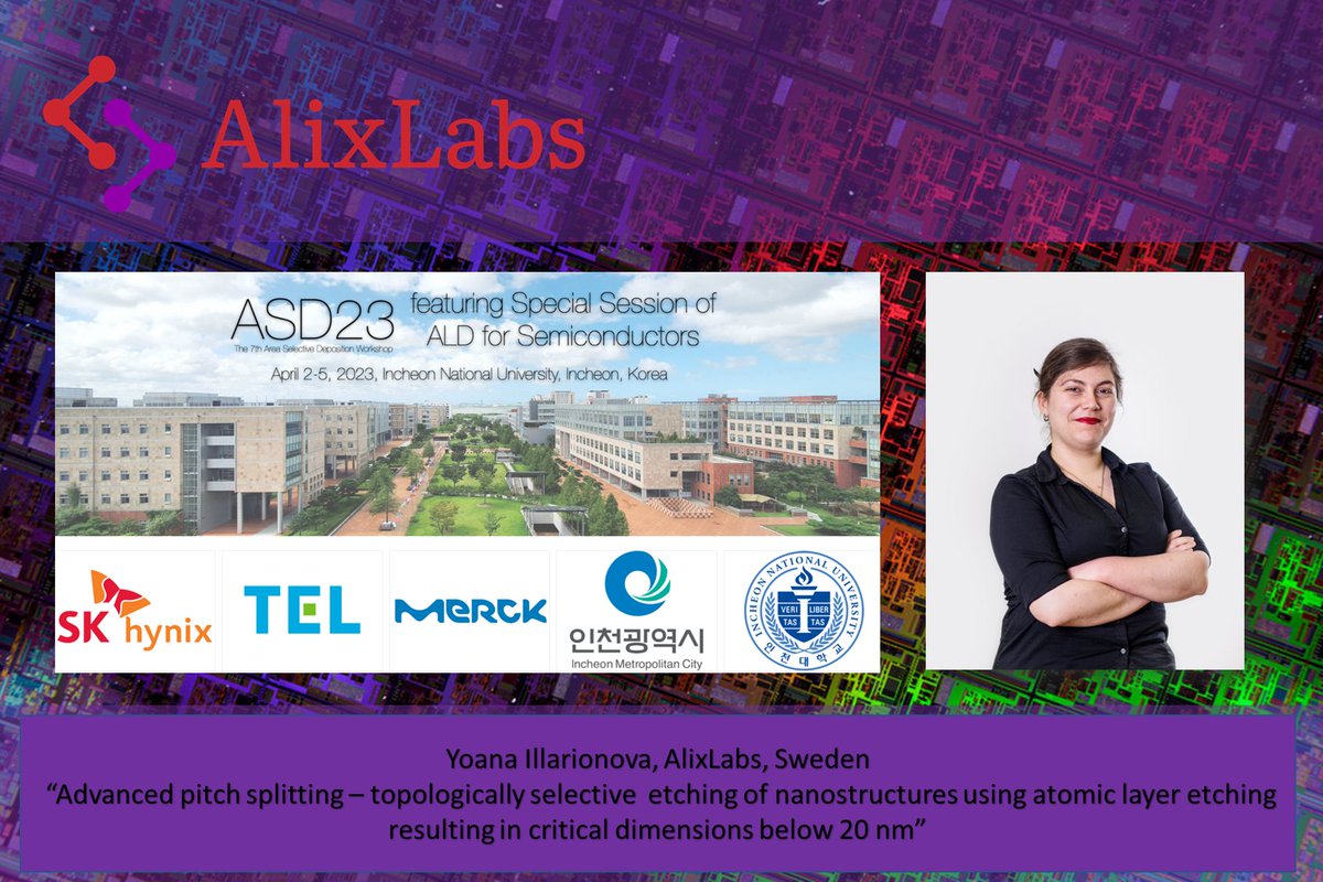
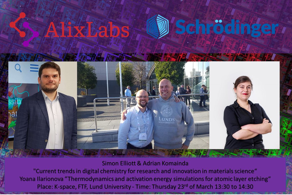
Mini-Symposium @Simon_D_Elliott & A.Komainda "Current trends in digital chemistry for research and innovation in materials science“ Y.Ilarionova “Thermodynamics and activation energy simulations for atomic layer etching“ @lunduniversity Thu. 23 March 13:30-14:30 #ALEtch #ALDep
0
2
2
Meanwhile, in Taipei Taiwan, our CEO Amin Karimi is busy introducing AlixLabs disruptive semiconductor manufacturing technology to the best of the best in Semiconductor manufacturing in The Taiwan Semiconductor Ecosystem. @TaiwanInSweden #Taiwan #Sweden @DrFrederickChen

0
1
4
RT @allpros_eu: Read the story of @AlixLabs, a Swedish startup that develops a new technology to reduce the number of steps needed to creat…
0
1
0
RT @arcticstartup: Swedish startup secures funding to develop energy-efficient technology for semiconductor manufacturing
0
3
0
RT @siliconvikings: #skanestartups @AlixLabs has recently secured €909K in funding to develop energy-efficient technology for semiconductor…
0
2
0
RT @beneqcorp: In #ALDStories, @jv3sund,CEO of AlixLabs, recalls when his team uncovered Atomic Layer Etch Pitch Splitting (APS), technolog…
0
4
0
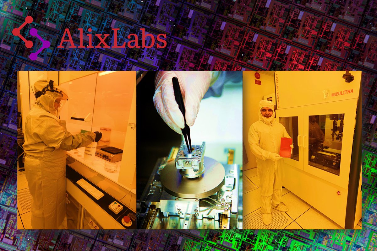
Using @Eulitha_AG Displacement Talbot Lithography (DTL) tool provided at @Lundsuni it is possible to produce critical feature sizes down to 60 nm with a DUV light source. We can go even further by employing AlixLabs APS technology, aiming at below 10 nm feature size #ALEtch
0
1
1
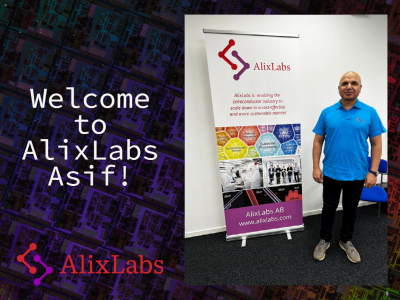
We start the new year 2023 at AlixLabs by welcoming Dr. Asif Mohammad joining AlixLabs today. Asif has a long experience in device fabrication and characterization. Welcome Asif!
0
0
0

RT @MobileHeights: ⚡️ How can Sweden and Europe supports its #semiconductor industry, and strengthens its resilience? Read our Position Pa…
0
5
0
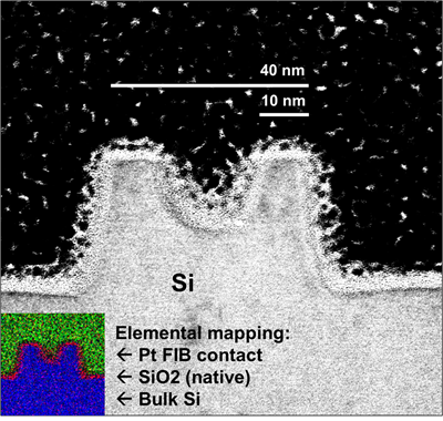
I Lund sker stordåd i små format, när AlixLabs demonstrerar etsning av nanostrukturer på bulkkisel. Nästa steg: att bevisa att processen är gångbar även på fullstora wafers.
0
1
2
RT @Semiconductor_T: First European patent for AlixLabs’ Atomic Layer Etch Pitch Splitting technique. @alixlabs
0
1
0

AlixLabs AB demonstrates pitch splitting in bulk silicon for leading edge semiconductor manufacturing
0
1
4