

Adam McCombs @[email protected]
@nanographs
Followers
4K
Following
11K
Statuses
9K
Find me on 🐘. Low key obsessed with open hardware 4 Electron Microscopes. Nanographs Co. is Isabel Burgos (@beamshift) and Adam McCombs. they/them
Portland, OR
Joined January 2014
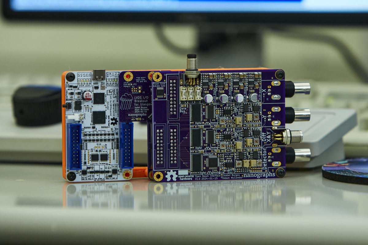
Introducing the first open source SEM digital image capture solution, the Open Beam Interface! GitHub: Bring your analog SEM into the digital world, all over one USB type-C connection. Taking orders now for our first batch of 6 boards, DM for details.
26
210
1K
@quantumbeans Sometimes said superglued parts are vacuum seals. One of those seals failed on a friend's TEM so he took it apart, scraped out all of the glue and re did it. For some reason the stage is about 1mm longer now so you can't get to the edge of the grid but def still a win.
0
0
10


Power strip from Amazon. Apparently the other 5 in the box have also melted/no longer work.


3
0
10
RT @Karly_Cohen: @Fishguy_FHL and I are running a bioimaging course at Friday Harbor Labs this winter! Focusing on CT, SEM, histology, phot…
0
25
0


0
6
0


RT @beamshift: For a quick check, hold a flat piece of aluminum foil in an ultrasonic cleaner for a minute and you can see where and how mu…
0
1
0
RT @QVHenkel: I wanted to see where the hotspots in my ultrasonic cleaner are and which water levels to avoid to get the most even pressure…
0
31
0
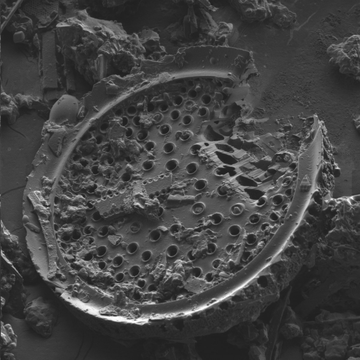
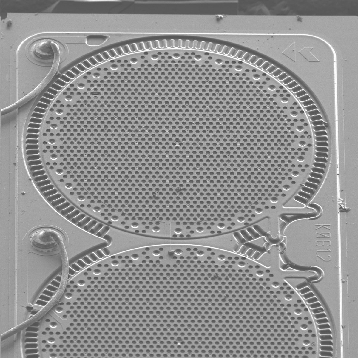
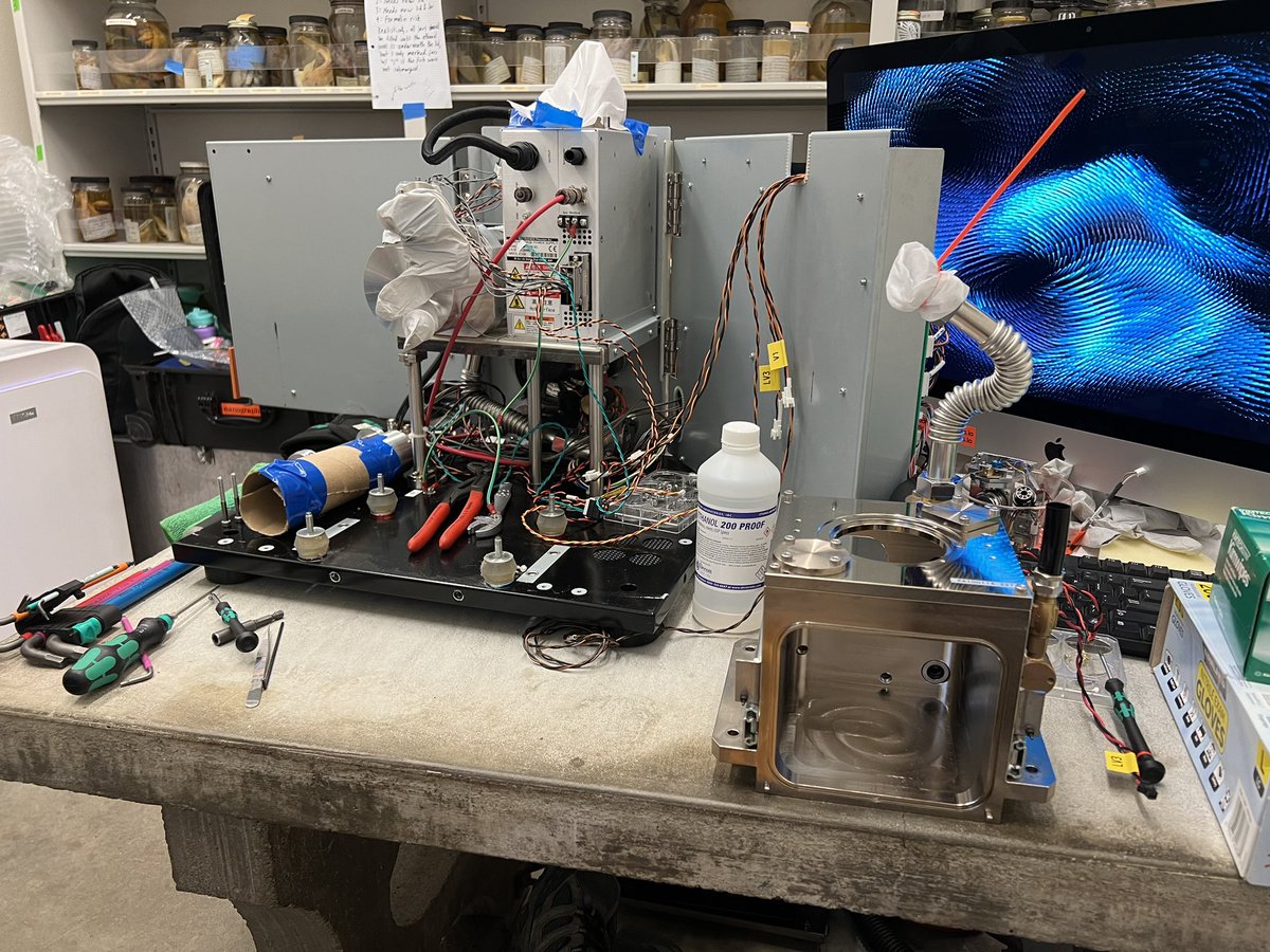
Look ma no chamber! Or column for that matter. Idk what happened but someone managed to get so much dust in this microscope that when @Fishguy_FHL went to blow it out a large cloud came out of the chamber 😳. Was so bad you couldn’t resolve an image at the lowest magnification.
3
0
17
RT @jwt0625: Just searched the whole notion workspace, "shit" appeared 54 times, and "piece of shit" appeared 25 times, 14 of which were wh…
0
1
0